Verified 2026-10
sparkfun Allband GNSS RTK Breakout - ZED-X20P (Qwiic)
All-band u-blox ZED-X20P-01B RTK breakout (GPS, Galileo, BeiDou, QZSS, NavIC plus L-band) with USB-C, an RT9080 3.3 V regulator, 19 through-hole pads, a BlueSMiRF header and a locking JST on UART2, two Qwiic sockets, and an SMA plus U.FL antenna footprint - I2C address 0x42, 3.3 V logic, 68 mA acquiring.
Place this board on a carrier in the editor →
Part & documents
| Data sheet | Data sheet → |
|---|---|
| Source | www.sparkfun.com/sparkfun-allband-gnss-rtk-breakout-zed-x20p-qwiic.html → |
Specs
| MCU | u-blox ZED-X20P-01B all-band GNSS receiver (GPS L1C/A, L2C, L5; Galileo E1-B/C, E5a, E6; BeiDou B1I, B1C, B2a, B3I; QZSS; NavIC; SBAS on L1C/A; L-band), with RTK, PPP-RTK and PPP positioning |
|---|
Pinout
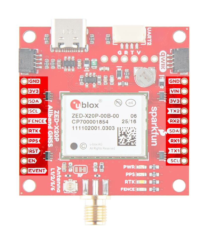
29 pads, as the vendor numbers them.
| # | Name | Function | Signals |
|---|---|---|---|
| 1 | GND | J3 pad 9: GND, common to the whole board | ground |
| 2 | VIN | J3 pad 8: VIN, 1.2-5.5 V into the RT9080-3.3 regulator (net VIN) | supply in, RT9080 regulator input |
| 3 | 3V3 | J3 pad 7: 3V3, the RT9080's regulated output, up to 600 mA (net 3.3V) | 3.3 V rail |
| 4 | TX2 | J3 pad 6: TX2, UART2 transmit, the RTCM/SPARTN correction port's output (net TX2) | UART2 transmit |
| 5 | RX2 | J3 pad 5: RX2, UART2 receive, corrections in (net RX2) | UART2 receive |
| 6 | SDA | J3 pad 4: SDA, I2C data on the module's SDA/SPI_CS_N pin (net SDA/!CS) | I2C data, SPI chip select when D_SEL is low |
| 7 | RX1 | J3 pad 3: RX1, UART1 receive and SPI_SDI in SPI mode (net RX1/PICO) | UART1 receive, SPI SDI when D_SEL is low |
| 8 | TX1 | J3 pad 2: TX1, UART1 transmit - the only port that can take a firmware update - and SPI_SDO in SPI mode (net TX1/POCI) | UART1 transmit, SPI SDO when D_SEL is low |
| 9 | SCL | J3 pad 1: SCL, I2C clock on the module's SCL/SPI_CLK pin (net SCL/SCK) | I2C clock, SPI clock when D_SEL is low |
| 10 | FENCE | J11 pad 1: FENCE, the module's GEOFENCE_STAT output, also driving the blue FENCE LED through R11 (2.2k) and jumper JP8 (net GEO_STAT) | geofence status output, blue FENCE LED |
| 11 | RTK | J11 pad 2: RTK, the module's RTK_STAT output - low when RTK fixed, blinking with corrections but no fix, high with no carrier-phase solution - also driving the white LED through R5 (2.2k) and JP3 (net RTK_STAT) | RTK status output, white RTK LED |
| 12 | PPS | J11 pad 3: PPS, the module's TIMEPULSE output, also driving the yellow PPS LED (net PPS) | time pulse output, yellow PPS LED |
| 13 | RST | J11 pad 4: RST, tied to the module's RESET_N; drive it LOW for at least 100 ms to cold-start the receiver and clear its configuration, RTC and orbit data (net RESET) | reset input, cold start |
| 14 | EN | J11 pad 5: EN, the RT9080's enable, active HIGH and pulled to the 5 V side by R9 (100k) so the rail comes up by default (net 3V3_EN) | 3.3 V regulator enable |
| 15 | EVENT | J11 pad 6: EVENT, the module's EXTINT input, used to wake the receiver from standby or to time-stamp an external event (net EVENT) | external interrupt input |
| 16 | GND | J9 pad 1: GND on the 4-pad I2C header (same ground net as J3) | ground |
| 17 | 3V3 | J9 pad 2: 3V3 on the 4-pad I2C header, the same regulated rail as J3 pad 7 | 3.3 V rail |
| 18 | SDA | J9 pad 3: SDA on the 4-pad I2C header, the same net as J3 pad 4 | I2C data |
| 19 | SCL | J9 pad 4: SCL on the 4-pad I2C header, the same net as J3 pad 1 | I2C clock |
| 20 | NC | J2 pad 1: NC, no connection in the schematic (unconnected-(J2-Pin_1-Pad1)) | not connected |
| 21 | TXD | J2 pad 2: TXD, UART2 transmit out of the board to a BlueSMiRF or serial link (net TX2) | UART2 transmit |
| 22 | RXD | J2 pad 3: RXD, UART2 receive into the board, through R8 (1k) as the HV-RX2 net | UART2 receive |
| 23 | 3V3 | J2 pad 4: 3V3, the rail the BlueSMiRF header runs from (net VOUT through JP4, bridged to 3V3 on delivery) | 3.3 V rail, also feeds JP4 VSEL |
| 24 | NC | J2 pad 5: NC, no connection in the schematic (unconnected-(J2-Pin_5-Pad5)) | not connected |
| 25 | GND | J2 pad 6: GND | ground |
| 26 | 3V3 | J8 pad 1: 3V3 on the locking JST, the VOUT net, which JP4 sets to 3V3 or 5V | UART2 JST supply, VSEL-selectable 3V3 or 5V |
| 27 | TXD | J8 pad 2: TXD, UART2 transmit for a telemetry radio such as the SiK Telemetry Radio V3 (net TX2) | UART2 transmit |
| 28 | RXD | J8 pad 3: RXD, UART2 receive, through R8 (1k) as the HV-RX2 net | UART2 receive |
| 29 | GND | J8 pad 4: GND | ground |
Buses
| Bus | Signals | Pins | Voltage | Note |
|---|---|---|---|---|
| I2C ×2 | SDA, SCL | SDA, SCL | 3.3 V V | 0x42, peripheral only, standard/fast/fast-mode-plus up to 1000 kbit/s with up to 20 ms clock stretching. The same two nets reach J3 pads 4 and 1, J9 pads 3 and 4 and both Qwiic sockets. The receiver runs I2C only while D_SEL is high; closing the SPI jumper takes I2C off these pins. 2.2 kOhm pull-ups R12 (SCL) and R13 (SDA) are fitted but reach 3.3 V only through JP9, which ships open. |
| SPI ×1 | SCLK, SDI, SDO, CS | SCL, RX1, TX1, SDA | 3.3 V V | Shares the UART1 and I2C pins and is disabled until the SPI jumper on the back (D_SEL) is closed; closing it also removes I2C. SCL becomes SPI clock, SDA becomes SPI chip select, RX1 becomes SPI_SDI and TX1 becomes SPI_SDO. SparkFun's table maps TX1 = SDO, RX1 = SDI, SDA = CS, SCL = CLK. The module is an SPI peripheral only. |
| UART ×1 | TX1, RX1 | TX1, RX1 | 3.3 V V | UART1 on J3 pads 2 (TX1) and 3 (RX1); 38400 baud 8N1 by default, 4800 to 8 Mbaud configurable. Firmware updates can only be done over UART1. |
| UART ×1 | TX2, RX2 | TX2, RX2 | 3.3 V V | UART2 is the RTCM/SPARTN correction port and is broken out twice: J3 pads 6 (TX2) and 5 (RX2), and both the J2 BlueSMiRF header and the J8 locking JST. Only one of those two connectors may be populated at a time. The RX line into J2/J8 passes through R8 (1k) as the HV-RX2 net. |
I²C / bus addresses
| Address | Bus | Device | Note |
|---|---|---|---|
| 0x42 | I2C | ZED-X20P-01B GNSS receiver | 7-bit address, given by SparkFun's hookup guide as 0x42 (1000010). There is no address strap or jumper on the board - the module's own configuration holds it - so a second receiver on the same bus needs its address changed in software before both will answer. |
Power
| Input | 1.2-5.5 V on VIN or 5 V over USB-C, into an RT9080 LDO |
|---|---|
| Input range | 1.2-5.5 V at VIN (RT9080 input); SparkFun recommends at least 3.5 V in for a clean 3.3 V output |
Module draw, measured at 3.3 V: 68 mA acquiring and 64 mA tracking with GPS+Galileo+BeiDou, 55 mA for GPS alone, and up to 85 mA peak during acquisition. 5 V is only needed for the USB interface, and when the VSEL jumper is set that way it also feeds the JST connector.
Outputs
| Rail | Rating | Note |
|---|---|---|
| 3.3V | 3.3 V V, 600 mA max | RT9080-3.3 regulator, up to 600 mA, enabled by the EN pad (active HIGH, enabled by default). Feeds the module, the LEDs, both Qwiic sockets, the BlueSMiRF header and the backup battery. |
Notes
Pads are numbered 1-29 here because the board's connectors each number their own pads from 1: J3 is a 1x09 (1-9), J11 a 1x06 (10-15), J9 a 1x04 (16-19), J2 the 1x06 BlueSMiRF header (20-25) and J8 the 1x04 locking JST (26-29). Every description names its connector and the vendor's own pad number. J3, J11 and J9 are the 19 through-hole pads SparkFun counts; their silkscreen labels were read off SparkFun's own header photograph and match the KiCad file's nets. The two Qwiic sockets (J4 and J7, JST-SH 1.0 mm 4-pin right-angle) carry the same four signals and are not numbered into `pins` because the vendor prints no per-pad label on them; each has two mechanical shield tabs the schematic marks NC. Test points TP1 (TX_READY), TP2 (V_BCKP) and TP4 (SAFEBOOT_N) are on the back and are not a connector. Eight solder jumpers sit on the back: PWR, PPS, RTK and FENCE (one per status LED, all bridged on delivery), I2C (JP9, open - bridge it to put the two 2.2 kOhm pull-ups on the bus), SPI (D_SEL), VSEL (JST VCC rail, bridged to 3V3 on delivery) and SHLD (USB-C shield to ground). part is null because SparkFun's own title already carries the module name, the same shape the Thing Plus entries took.
AI context
Dense context for pasting into a model prompt — addresses, pinout, voltages, tolerances and the vendor's reference circuit.
PART: SparkFun Allband GNSS RTK Breakout - ZED-X20P (Qwiic), GPS-28871, 43.2 mm x 43.2 mm (1.70 in square) with four 4-40 mounting holes, built around a u-blox ZED-X20P-01B all-band GNSS module (17.0 mm x 22.0 mm x 2.4 mm). The board adds a USB-C receptacle, an RT9080-3.3 3.3 V regulator, 19 through-hole pads, two Qwiic sockets, a 6-pad BlueSMiRF header and a 4-pad locking JST (both on UART2), an SMA connector with a U.FL alternative behind a jumper, a rechargeable backup battery, and PWR/PPS/RTK/FENCE LEDs. Constellations: GPS L1C/A L2C L5, Galileo E1-B/C E5a E6, BeiDou B1I B1C B2a B3I, QZSS L1C/A L1C/B L2C L5, NavIC L1 L5, SBAS on L1C/A, plus L-band corrections handled on the module itself.
I2C: 7-bit address 0x42, peripheral only, standard/fast/fast-mode-plus up to 1000 kbit/s, clock stretching up to 20 ms, 400 pF per bus line (550 pF in fast-mode-plus). There is no address strap on the board, so two receivers on one bus must be given different addresses in software.
PINOUT: J3 (1x09) pad 1 SCL, 2 TX1, 3 RX1, 4 SDA, 5 RX2, 6 TX2, 7 3V3, 8 VIN, 9 GND. J11 (1x06) pad 1 FENCE, 2 RTK, 3 PPS, 4 RST, 5 EN, 6 EVENT. J9 (1x04, I2C) pad 1 GND, 2 3V3, 3 SDA, 4 SCL. J2 (1x06, BlueSMiRF) pad 1 NC, 2 TXD, 3 RXD, 4 3V3, 5 NC, 6 GND. J8 (1x04, locking JST) pad 1 3V3, 2 TXD, 3 RXD, 4 GND. Both Qwiic sockets are pad 1 GND, 2 3V3, 3 SDA, 4 SCL. On J3 the I2C names sit on pads 1 and 4 while the same pins are SPI clock and SPI chip select when D_SEL is low; RX1 and TX1 become SDI and SDO.
SUPPLY: VIN takes 1.2-5.5 V and the RT9080-3.3 makes the 3.3 V rail at up to 600 mA; SparkFun recommends at least 3.5 V at VIN for a clean 3.3 V output. The module itself runs 2.7-3.6 V (3.3 V typical). Draw at 3.3 V is 68 mA acquiring and 64 mA tracking on GPS+Galileo+BeiDou, 55 mA on GPS alone, with peaks to 85 mA during acquisition - size the feed for that. 5 V is only needed for USB, and only when the VSEL jumper selects it does the JST's VCC pin carry 5 V.
LOGIC: 3.3 V, all PIOs referenced to VCC. Absolute maximum VCC -0.3 to 3.6 V, any digital IO pin -0.3 V to VCC+0.3 V with a 3.6 V ceiling, source or sink 10 mA per pin, RF_IN -5.5 to +5.5 V DC and +15 dBm; the module has no overvoltage or reverse-voltage protection, so a 5 V host will damage it. Internal pull-ups: 8-40 kOhm on SCL, SDA, RXD2, TXD2, TIMEPULSE, TX_READY and the antenna pins, 35-205 kOhm on D_SEL, RXD, TXD, SAFEBOOT_N, EXTINT, GEOFENCE_STAT and RTK_STAT, 7-13 kOhm on RESET_N. Unused inputs can be left open.
REFERENCE CIRCUIT: 3.3 V carries C2 10 uF, C5 0.1 uF and C8 33 pF; V_BCKP has C9 1 uF plus the backup cell; the antenna rail VCC_RF is fed through R6 10 Ohm with C3 0.1 uF to ground. I2C pull-ups R12 (SCL) and R13 (SDA) are 2.2 kOhm and reach 3.3 V only through JP9, a 3-pole solder jumper that ships open - bridge pad 1-2 and pad 2-3 to put them on the bus. J2/J8 RXD passes through R8 1k. Each status LED has its own cuttable jumper (PWR, PPS, RTK, FENCE).
TRAPS: RST held LOW for 100 ms or more is a cold start that erases configuration, RTC and orbit data, and a capacitor from RST to GND re-triggers a reset on every power-up, so fit none. SAFEBOOT_N and TIMEPULSE are joined inside the module by a 1 kOhm series resistor, so anything loading the PPS pad low at startup drops the receiver into safeboot mode. Firmware updates only over UART1. The BlueSMiRF header and the JST are the same UART2 - populate one, not both, or the two drivers contend. The UART receiver turns itself off when it counts more than 100 framing errors in one second, which is what a wrong baud rate or a grounded RX line produces. SPI is off until the D_SEL jumper is closed, and closing it removes I2C from those pins. The U.FL connector only works after the RF jumper moves the antenna path off the SMA. Defaults: UART1 NMEA at 38400 8N1, UART2 RTCM 3.4 out and RTCM/SPARTN in with NMEA disabled, UART2 also carries UBX.
Provenance
Every figure on this page was read from the 5 sources below and last checked on Oct 23, 2026.
- vendor SparkFun - Allband GNSS RTK Breakout - ZED-X20P (Qwiic) product page (GPS-28871, $299.95 USD; ZED-X20P-01B module; 19 PTH pins, 2x Qwiic, 3 UART interfaces, USB-C; 2.7-3.6 V module supply; four status LEDs; backup battery)
- reference SparkFun ZED-X20P GNSS Breakout hookup guide, Hardware Overview (VIN 1.2-5.5 V, RT9080 600 mA, 3.5 V recommended input, I2C address 0x42, BlueSMiRF and JST pin tables, power consumption table, jumper list, RESET_N and SAFEBOOT_N traps)
- image SparkFun ZED-X20P breakout header photograph (the 19 through-hole pad labels: GND VIN 3V3 TX2 RX2 SDA RX1 TX1 SCL on J3, GND 3V3 SDA SCL on J9, FENCE RTK PPS RST EN EVENT on J11)
- datasheet u-blox ZED-X20P-01B data sheet UBXDOC-304424225-21281 (absolute maximum ratings, VCC 2.7-3.6 V, digital IO limits and internal pull-up values, current consumption, I2C/SPI/UART/D_SEL behaviour, RF_IN limits)
- datasheet SparkFun GNSS ZED-X20P KiCad design files (J3/J11/J9/J2/J8 pad nets, R12/R13 2.2k I2C pull-ups, JP9 open 3-pole I2C jumper, JP4 VSEL bridged to 3V3, RT9080-3.3 U2, C2 10uF, C5 0.1uF, C8 33pF, C3 0.1uF + R6 10R on VCC_RF, C9 1uF on V_BCKP, R8 1k on the HV-RX2 line)