Verified 2026-10
SparkFun Thing Plus - RP2350
Thing Plus (Feather-footprint) RP2350A board with a Raspberry Pi RM2 radio on the Pico W's SPI pins, 16 MB QSPI flash, 8 MB PSRAM, a microSD slot, Qwiic, a 214 mA LiPo charger with a MAX17048 fuel gauge, and 21 GPIO on the two 0.1in headers - 3.3 V logic throughout.
Place this board on a carrier in the editor →
Specs
| MCU | Raspberry Pi RP2350A (dual Arm Cortex-M33 or dual Hazard3 RISC-V, user-selectable at boot, 150 MHz, 520 KB SRAM in 10 banks, 8 KB OTP) plus a Raspberry Pi RM2 radio module (2.4 GHz WiFi 4 802.11n, Bluetooth 5.2 LE and Classic) |
|---|---|
| Clock | 150 MHz |
| Flash | 16 MB |
| RAM | 520 KB |
| I/O | 21 digital, 3 analog, 24 PWM |
SparkFun's own count for the header: 21 GPIO broken out, of which 3 are analog-capable (GPIO26/27/28). The RP2350A silicon has 30 5 V-tolerant GPIO and 4 analog inputs; 24 PWM channels, 2 UART, 2 SPI, 2 I2C and 12 PIO state machines are muxed onto the GPIO, so the header pins are GPIO rather than fixed functions. Eight GPIO numbers are consumed on-board and are not on the header: GPIO2/3/4 (µSD, shared with the exposed SPI), GPIO13 (3.3V_P regulator enable), GPIO14 (WS2812 data in), and the RM2's SPI/control pins.
Pinout
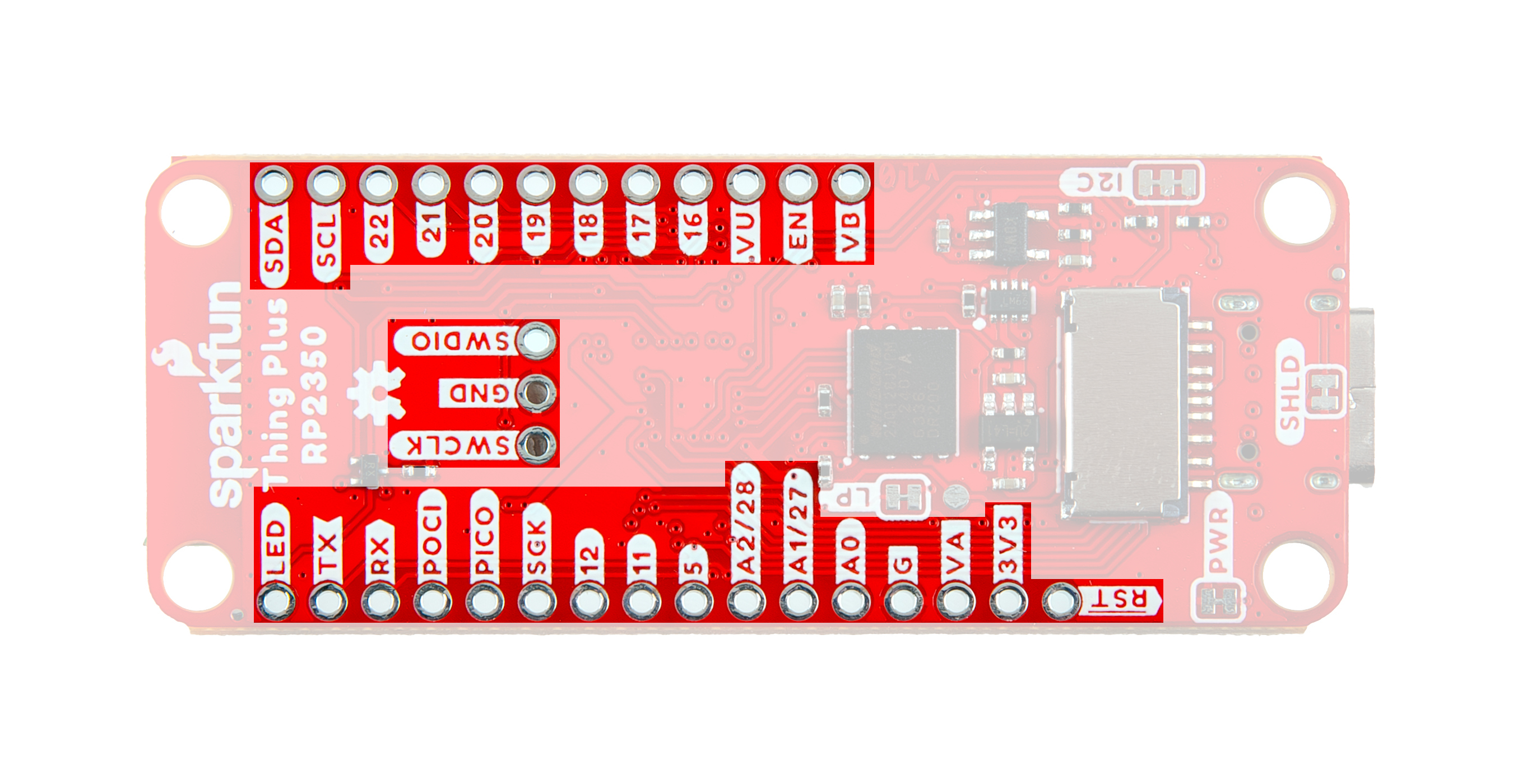
28 pads, as the vendor numbers them.
| # | Name | Function | Signals |
|---|---|---|---|
| 1 | SDA | GPIO6 - I2C data. Also the SDA line of the Qwiic connector; 2.2k to 3.3V through the I2C solder jumper, closed by default | GPIO6, I2C SDA |
| 2 | SCL | GPIO7 - I2C clock. Also the SCL line of the Qwiic connector; 2.2k to 3.3V through the I2C solder jumper, closed by default | GPIO7, I2C SCL |
| 3 | 22 | GPIO22, brought out plain | GPIO22 |
| 4 | 21 | GPIO21, brought out plain | GPIO21 |
| 5 | 20 | GPIO20, brought out plain | GPIO20 |
| 6 | 19 | GPIO19, brought out plain | GPIO19 |
| 7 | 18 | GPIO18, brought out plain | GPIO18 |
| 8 | 17 | GPIO17, brought out plain | GPIO17 |
| 9 | 16 | GPIO16, brought out plain | GPIO16 |
| 10 | VU | V_USB - direct to the USB-C VBUS and the MCP73831 charger input. Do not exceed 5.5 V here | 5 V supply in, charger input |
| 11 | EN | Enable of the main 3.3 V regulator (U3); the fab file's net is EN | regulator enable |
| 12 | VB | V_BATT - direct to the JST battery connector and the charger output, not regulated | battery in/out |
| 13 | LED | The 'FREEBIE' pad: the DATA OUT of the on-board WS2812, for daisy-chaining more LEDs. Not a GPIO | WS2812 data out |
| 14 | TX | GPIO0 - UART transmit | GPIO0, UART TX |
| 15 | RX | GPIO1 - UART receive | GPIO1, UART RX |
| 16 | POCI | GPIO4 - SPI controller-in/peripheral-out (MISO). Shares the bus with the µSD slot | GPIO4, SPI MISO |
| 17 | PICO | GPIO3 - SPI controller-out/peripheral-in (MOSI). Shares the bus with the µSD slot | GPIO3, SPI MOSI |
| 18 | SCK | GPIO2 - SPI clock. Shares the bus with the µSD slot | GPIO2, SPI SCK |
| 19 | 12 | GPIO12, brought out plain | GPIO12 |
| 20 | 11 | GPIO11, brought out plain | GPIO11 |
| 21 | 5 | GPIO5, brought out plain | GPIO5 |
| 22 | A2/28 | GPIO28 - also ADC2. Silk prints both the analog name and the MCU pin number | GPIO28, ADC2 |
| 23 | A1/27 | GPIO27 - also ADC1 | GPIO27, ADC1 |
| 24 | A0 | GPIO26 - also ADC0. The one analog pin printed without its MCU number | GPIO26, ADC0 |
| 25 | G | Ground | ground |
| 26 | VA | The analog reference position on the Feather header. On this board the fab file ties it to the VDDA net, which is the RP2350 ADC_IOVDD supply, so it is a 3.3 V reference tap rather than a pin you drive | ADC supply / AREF |
| 27 | 3V3 | Regulated 3.3 V out of the main regulator, 500 mA maximum | 3.3 V out |
| 28 | RST | RP2350 RUN - active-low reset. R12 pulls it up, and the RESET button shorts it to ground | reset, RUN |
Buses
| Bus | Signals | Pins | Voltage | Note |
|---|---|---|---|---|
| I2C ×1 | SDA, SCL | SDA, SCL | 3.3 V | GPIO6/GPIO7. Shared by header pads 1-2, the Qwiic connector and the MAX17048 fuel gauge. Both lines carry 2.2k pull-ups to 3.3 V through the three-way I2C jumper, which is closed by default. |
| SPI ×1 | SCK, PICO, POCI | SCK, PICO, POCI | 3.3 V | GPIO2/3/4 on header pads 18/17/16, using Raspberry Pi Pico naming (PICO = MOSI, POCI = MISO). The µSD slot hangs off the same three lines plus its own chip select, so an SD card and an SPI peripheral share one bus. |
| UART ×1 | TX, RX | TX, RX | 3.3 V | GPIO0/GPIO1 on pads 14/15. |
| USB ×1 | D+, D- | 5 V | USB-C, RP2350's USB 1.1 controller, also the bootloader port and the 5 V input. |
I²C / bus addresses
| Address | Bus | Device | Note |
|---|---|---|---|
| 0x36 | I2C | MAX17048 fuel gauge | Fixed in silicon; the board straps nothing, so it cannot be moved. The datasheet's prose gives the address as 0x6C write / 0x6D read, which is the 8-bit form including the R/W bit; its own address diagram in the same section reads 0110110, i.e. 0x36 as a 7-bit address, which is what a Linux or Arduino scan will report. It sits on the same GPIO6/GPIO7 bus as the header and the Qwiic connector, so a Qwiic device at 0x36 would collide. |
Power
| Input | USB-C 5 V, or a single-cell LiPo on the 2-pin JST connector, or 5 V straight onto the VU pad |
|---|---|
| Input range | 5 V USB (VU must not exceed 5.5 V); battery direct to VB |
The MCP73831 charger is rated 214 mA at 3.3 V and is fed from V_USB, so it only charges while 5 V is present on USB or the VU pad. A MAX17048 fuel gauge sits on the I2C bus to report battery state. SparkFun publishes no overall board current draw, so none is recorded here. Two board revisions exist: v10 (DD-27675) has the LiPo JST polarity REVERSED from SparkFun's norm and is incompatible with every single-cell LiPo they sell; v11 (WRL-25134, the SKU queued here) fixes it. Check the silkscreen before plugging a battery into any board of unknown revision.
Outputs
| Rail | Rating | Note |
|---|---|---|
| 3V3 | 3.3 V, 500 mA max | Main regulator, 500 mA at 3.3 V per SparkFun |
| 3.3V_P | 3.3 V | Second RT9080 regulator feeding the Qwiic connector, the µSD slot and the WS2812. On by default via the LP jumper; its enable is GPIO13, so opening the jumper hands that rail to code. |
Notes
Pin numbers 1-28 are the fab file's own J1 pad numbers in the THING_PLUS package: 1-12 are one row, 13-28 the other. Rows run in opposite directions - pad 1 (SDA) and pad 13 (LED) are at the same end of the board, and the numbers climb away from that end on both sides. That is NOT the Adafruit Feather order, so do not assume a Thing Plus footprint and a Feather footprint share a pin numbering: the pads land in the same physical places, the numbers do not. Silk labels come from SparkFun's own pinout photo, cross-checked against the fab file's nets: the GPIO pins are printed as bare numbers (22, 21, 20 ... 16, 12, 11, 5), the analog ones as A2/28, A1/27 and A0, and the rest as SDA, SCL, VU, EN, VB, LED, TX, RX, POCI, PICO, SCK, G, VA, 3V3, RST. PICO is MOSI and POCI is MISO (Pico naming, not the usual MOSI/MISO words). The centre row of three pads is a SWD debug header labelled SWDIO / GND / SWCLK - SparkFun prints no pin numbers on it, so it is described here rather than numbered into `pins`. The VA pad is at the Feather AREF position and the schematic symbol even names it AREF/NC, but the board netlist puts it on VDDA, the ADC_IOVDD supply, so it is a reference tap and not a free pin. The WS2812's data IN is GPIO14, which is internal only; the pad labelled LED is its data OUT, so a WS2812 chain is fed from pad 13 and the first LED on the board cannot be addressed separately. Warning from the hookup guide worth repeating: keep the SPI lines LOW while the µSD card is unpowered - driving them high in that state can damage the GPIO. Four solder jumpers: PWR (power LED, closed), I2C (the 2.2k pull-ups, closed), LP (peripheral rail always-on, closed), SHLD (USB shield to ground, closed). Board is 58.42 x 22.86 mm with four 4-40 mounting holes, and the RM2 antenna sits very close to the two holes at the USB end.
Provenance
Every figure on this page was read from the 6 sources below and last checked on Oct 20, 2026.
- vendor SparkFun - Thing Plus RP2350 product page (WRL-25134, $30.95; 21 GPIO, 28 PTH pins, 16 MB flash, 8 MB PSRAM, MCP73831 charger, MAX17048 fuel gauge, 2.3 x 0.9 in, USB-C, Qwiic, µSD)
- reference SparkFun hookup guide - Hardware Overview (500 mA at 3.3 V regulator, 214 mA charge rate, Qwiic on GPIO6/GPIO7, RT9080 peripheral regulator enabled by GPIO13, WS2812 data in on GPIO14 and FREEBIE as its data out, 2.2k I2C pull-ups, v10 reversed JST polarity, 58.42 x 22.86 mm, keep SPI low with the SD card unpowered)
- datasheet SparkFun Thing Plus RP2350 schematic PDF (J1 pin names and nets: SDA/SCL on GPIO6/7, TX/RX on GPIO0/1, SCK/PICO/POCI on GPIO2/3/4, A0/A1/A2 on GPIO26/27/28, VDDA on the VA pad, RUN on RST with R12 pull-up, EN on the regulator)
- datasheet SparkFun Thing Plus RP2350 Eagle fab file (element J1, package THING_PLUS: pads 1-28 in two rows, pad 1 SDA and pad 13 LED at the same end; net per pad used for every pin number above)
- reference SparkFun - Thing Plus RP2350 pinout photo (the silkscreen labels read off the vendor's own image: SDA, SCL, 22-16, VU, EN, VB one row; LED, TX, RX, POCI, PICO, SCK, 12, 11, 5, A2/28, A1/27, A0, G, VA, 3V3, RST the other; centre SWDIO/GND/SWCLK)
- datasheet SparkFun - MAX17048 datasheet (I2C fuel gauge, fixed 7-bit address 0x36)